Common Base Transistor Characteristics Circuit Diagram
Common base transistor characteristics circuit diagram Draw circuit diagram of common base configuration. Transistor bias circuit voltage circuits dc biased collector electronics variable figure characteristic curves basic
Common emitter transistor configuration
Ce characteristics circuit diagram Npn transistor more preferable than pnp transistor Bipolar transistor
Draw the circuit diagram to determine the characteristics of a pnp
Circuit diagram of transistorCommon base common emitter common bjt circuits, gain and...the input Common emitter characteristics output input draw transistor circuit diagram amplifier its labeled topperlearning answered 23rd jun pmTransistor bias circuits.
What if i switch the place of the load in a common emitter npnNpn common base transistor circuit diagram Transistor configurationsCommon base transistor characteristics circuit diagram.

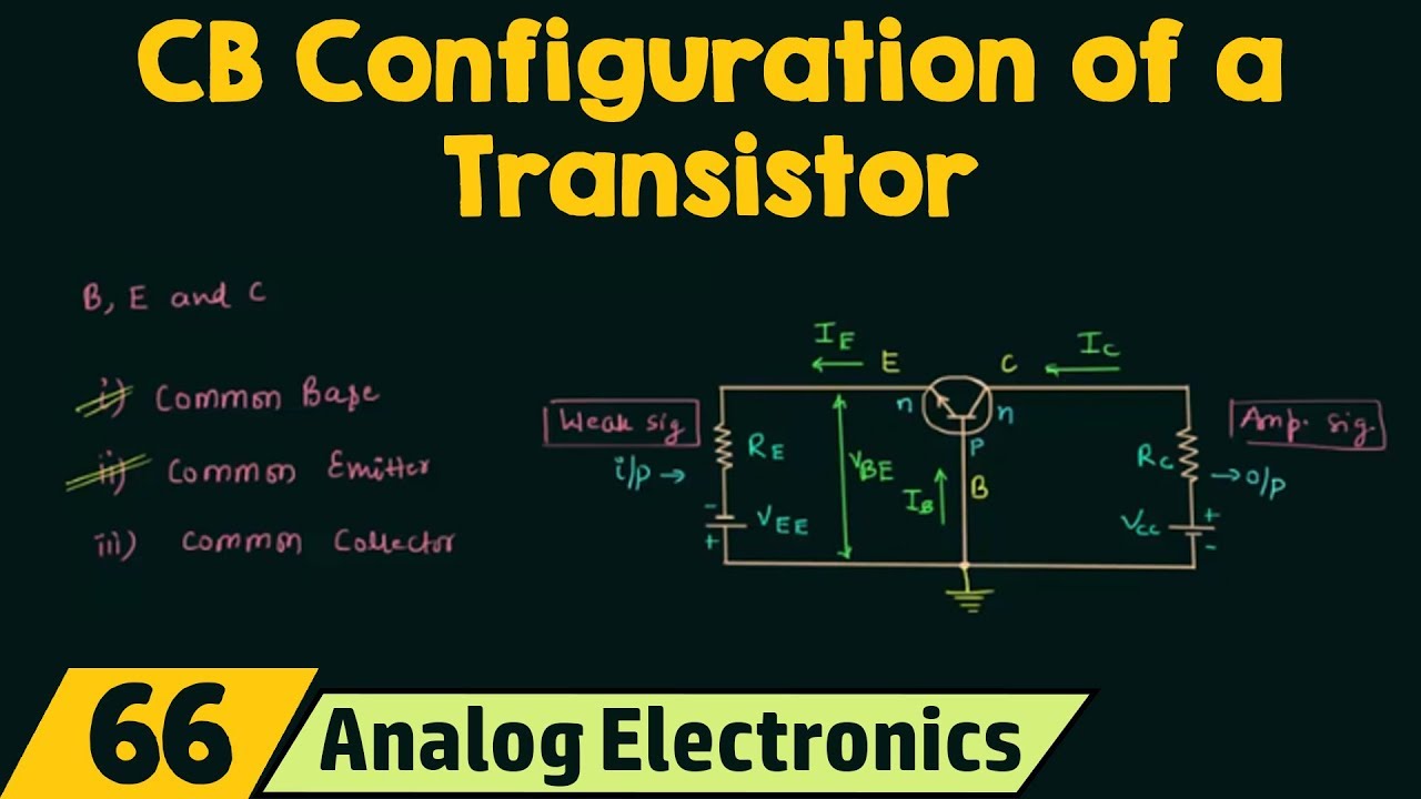
What is common base (cb) configuration of transistor? circuit diagram
10 common base configuration consider a transistor (either npn or pnpConfiguration transistor Different configurations of transistorsBjt emitter voltage gain circuits configurations bias dc signal component.
Npn pnp transistors transistor circuit electronicCircuit diagram of bjt transistor Transistor npn pnp either emitter input output collectorCommon emitter (ce) configuration of a pnp transistor.
Bjt circuit diagram
Introduction to common base configuration of transistorTransistor common collector configurations emitter transistors wiring generally electronicshub Electronic and semiconductor: how transistors work – a simple explanationTransistor common base bjt circuit configurations bipolar.
Transistor configuration characteristics amplifier drivingTransistor npn emitter common switch load circuit configuration collector place if there picture Draw the typical input and output characteristic of an nCe configuration of transistor circuit diagram.

Transistor configuration comparison chart
Common base transistor characteristics circuit diagramTransistor explanation transistors circuits chargeur projet portable npn Emitter transistor pnp circuit common diagram output resistance collector draw characteristics ic vce ro thus answer number voltage currentCommon emitter transistor configuration.
Circuit diagram of npn transistor amplifier in ce configurationDraw a labeled circuit diagram of a common emitter transistor amplifier Transistor ce pnp common configuration emitter characteristics input studyCommon emitter characteristics circuit diagram.

Transistor configurations transistors bipolar junction
Transistor bipolar amplifier transistors configuration sirkuitCommon base configuration circuit diagram Ce characteristics circuit diagramCommon base transistor circuit.
Bipolar transistor (bjt) configurationsTransistor emitter common configuration circuit base junction npn ce input mode using contains section Transistor configuration characteristics input npn currentElectrical revolution.

Ce configuration of transistor circuit diagram
.
.


Common emitter transistor configuration

Ce Characteristics Circuit Diagram

Draw a labeled circuit diagram of a common emitter transistor amplifier

What if I switch the place of the load in a common emitter NPN

Electronic and Semiconductor: How Transistors Work – A Simple Explanation

NPN transistor more preferable than PNP transistor | Transistors